Scanning Electron Microscopy (SEM) Inspection
 Scanning Electron Microscopy Inspection (SEM)
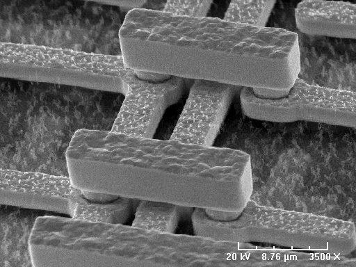
SEM images are produced by scanning a focused electron beam across the surface of a specimen. In the SE image mode, the low energy secondary electrons emitted are detected and used to modulate the brightness of a synchronously scanned CRT. Other emitted signals, such as X-rays, can also be detected and used to characterize the specimen. These X-rays energies are characteristic of the elemental composition of the specimen area probed by the primary electron beam allowing both a qualitative and quantitative determination of the elements. High energy back-scattered electrons (BSE) can be also be detected. Since the back-scattering emission efficiency is a function of atomic weight (density) which varies with elemental composition the image contrast can be exploited providing elemental spatial information.
Information Obtained
- Surface topography if low energy secondary electrons are collected
- Atomic number or orientation information if higher energy backscattered electrons are used for imaging
- Differentiation between surface roughness, porosity, granular deposits, stress-related gross microcracks (often used in conjunction with microsectioning)
- Observation of grain boundaries in unetched samples
- Critical dimension measurements
- Elemental Analysis
ORS holds DLA Suitability for SEM Metal Inspection per MIL-STD 750, Method 2077 & MIL-STD 883, Method 2018
Sensitivity and Resolution
- Lateral resolution for SEM: < 100Å
- Lateral Resolution for EDX: 1 µm
- Detection limits for EDX: 0.5 – 1% atomic
Instrumentation
- Hitachi 6600 Variable Pressure FE-SEM IXRF Systems Model 550i – Silicon Drift Detector Elemental Mapping, SEI, BSE digital imaging
- JEOL 820i Scanning Electron Microscope with Kevex light element Quantum Energy Dispersive X-Ray Analyzer, Digital Elemental Imaging, Backscattered Electron Detection
- Cambridge Stereoscan 360 Scanning Electron Microscope with 40kV LaB6 Emitter
- JEOL JSM-6060LV Variable Pressure Electron Microscope with Noran Six-Sigma EDS
Advantages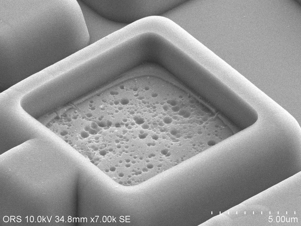
- Fast, relatively inexpensive near-surface screening method
- Depth of field is better than optical microscopy or transmission electron microscopy
