Acoustic Microscopy
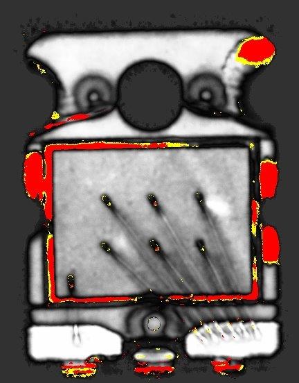
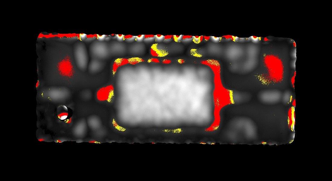 Acoustic Microscopy is a non-destructive screening technique offering unique insight on the integrity of package and device construction. Its advantages include the detection of void formations, delaminations, cracks and fractures as well as other hidden internal defects within inherently susceptible materials and device types. Various device types like SOIC’s, BGA’s, CSP’s, encapsulating materials, PCB’s, molding compounds, flex circuits, and other products may be analyzed. Testing performed to IPC/JEDEC J-STD-035, Acoustic Microscopy for Nonhermetic Encapsulated Electronic Components, or client requirements.
A high frequency ultrasound transducer emits sound waves that can be received back (echo) or transmitted through a material. The acoustic signature or waveform may then be interpreted to determine variations of acoustic impedance within a sample. The difference in acoustic impedance may indicate a change in material densities or separation at an interface. The transducer may also be mechanically scanned across the sample in a raster pattern emitting and receiving the ultrasound signal to generate an image (pulse-echo). An immersion fluid medium, typically DI water, is used to acoustically couple the sample while performing the analysis.
Measurement Modes
- A-Scan: The A-Scan mode is used to characterize a single point of interest in a specimen. It is also used as a convenient method of focusing the microscope.
- B-Scan: The B-Scan mode generates a top-down or X-Z axis cross-sectional image of the sample. Tilted artifacts or features and non-planar fracture propagations can be identified.
- C-Scan: The C-Scan mode or pulse-echo provides a planar view image at a specific depth. Illustrations of delaminations and void formation can be generated.
- Through-Scan: Through-Scan transmission mode generates images based on variations in acoustic impedance. This mode is often necessary to verify defects observed during C-Scan mode analysis.
 Applications
- Ceramic Capacitor Defects
- Plastic Package Defects
- Die Attach Defects
- Pharmaceutical and Medical Package Defects
- Flip Chips
- Chip Scale Packages (CSP)
- Ball Grid Arrays (BGA)
- Metal Ball Grid Arrays (MBGA)
- Plastic Encapsulated IC’s
- Hybrids
- Multi-Chip Modules (MCM)
- Bonded Wafers
